

| 欧盟限制某些有害物质的使用 | Compliant |
| ECCN (US) | EAR99 |
| Part Status | Active |
| HTS | 8541.29.00.95 |
| 产品类别 | Power MOSFET |
| Process Technology | TrenchFET |
| Configuration | Dual |
| Channel Mode | Enhancement |
| Channel Type | P|N |
| Number of Elements per Chip | 2 |
| Maximum Drain Source Voltage (V) | 30 |
| Maximum Gate Source Voltage (V) | ±20 |
| Maximum Gate Threshold Voltage (V) | 2.6 |
| Maximum Continuous Drain Current (A) | 0.85 |
| Maximum Gate Source Leakage Current (nA) | 100 |
| Maximum IDSS (uA) | 1 |
| Maximum Drain Source Resistance (mOhm) | 940@10V@P Channel|280@10V@N Channel |
| Typical Gate Charge @ Vgs (nC) | 1@4.5V@N Channel|1.2@4.5V@P Channel |
| Typical Input Capacitance @ Vds (pF) | 38@15V@N Channel|40@15V@P Channel |
| Maximum Power Dissipation (mW) | 1500 |
| Typical Fall Time (ns) | 17@P Channel|32@N Channel |
| Typical Rise Time (ns) | 39@P Channel|18@N Channel |
| Typical Turn-Off Delay Time (ns) | 8@N Channel|10@P Channel |
| Typical Turn-On Delay Time (ns) | 3@N Channel|4@P Channel |
| Minimum Operating Temperature (°C) | -55 |
| Maximum Operating Temperature (°C) | 175 |
| Supplier Temperature Grade | Automotive |
| Automotive | Yes |
| AEC Qualified Number | AEC-Q101 |
| Pin Count | 6 |
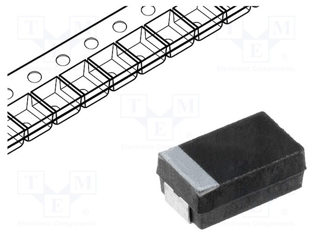
| Supplier Package | SC-70 |
| Military | No |
| Mounting | Surface Mount |
| Package Height | 1(Max) |
| Package Length | 2 |
| Package Width | 1.25 |
| PCB changed | 6 |
 种类齐全 一站购物
 正品保障 源头可溯
 极速物流 在线跟踪
 优质服务 省心省时
 客服企业微信